
Solution
FPGA to ASIC Conversion
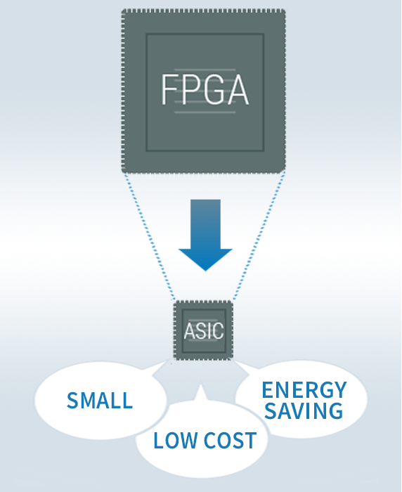
We reduce cost in mass production by changing FPGAs to ASICs.
While FPGAs can keep the initial cost lower than ASICs, it is more costly when a large volume of mass production is required. To reduce costs, it is essential to select FPGAs or ASICs according to the quantity required. MegaChips provides maximum support to customers in converting FPGAs to ASICs.
Difference between FPGAs and ASICs
Making a judgment for converting FPGAs to ASICs is based on power consumption as well as cost. Recent advances in FPGA process miniaturization have greatly increased the number of logics that can be mounted and improved the operating frequency. On the other hand, the problem of increasing power consumption, in particular leakage power, causes FPGAs to become overheated. The most important recent issue for FPGAs is to increase operating frequency. This is because it is impossible to implement a low-power design such as a clock gating insertion and multi-Vth optimization, which are becoming a norm in ASICs. Applying FPGAs may require additional thermal measures, such as mounting the heatsink on the package, which may further increase the cost of mass production.
ASICs have a higher gate usage efficiency than FPGAs with similar processes, so power consumption can be reduced by converting FPGAs to ASICs or applying a low-power design method. In addition, the operating speed for FPGAs is slower than ASICs, so ASICs of a previous-generation process can support the operating speed of FPGAs. Converting FPGAs to ASICs with the process of a previous generation can be expected to reduce power usage by over two-thirds.
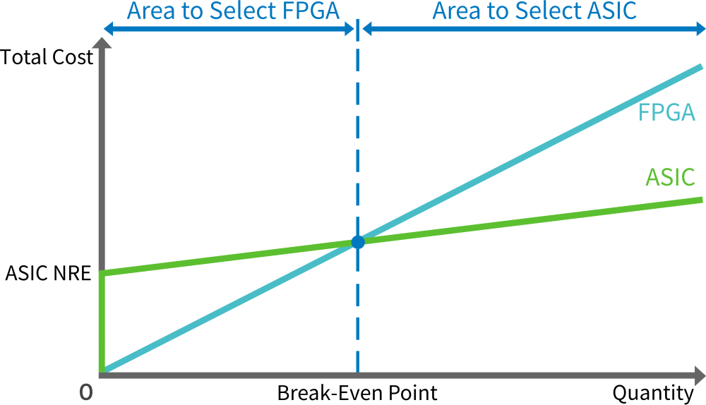
The following table shows the advantages and disadvantages when comparing FPGAs and ASICs. From the standpoint of the impact on initial cost, time to market, and ECO , it is better to apply FPGAs. However, if the mass production volume is large, selecting ASICs can save costs. The chart below shows the balance between the volume and cost for FPGAs and ASICs.
Comparison of FPGAs and ASICs
| Category | Item | FPGA | ASIC |
| Initial cost/Time to market | Logic design period | Excellent | Excellent |
| Layout period | Excellent | Good | |
| Manufacturing period | Excellent | Poor | |
| Cost of reticle | - | Poor | |
| Risk of development/Impact of ECO schedule | Iteration period due to logic correction after tape-out | Excellent | Poor |
| Cost of reticle due to logic correction after tape-out | - | Poor | |
|
Performance/Cost/Others |
Operation frequency | Good | Excellent |
| Degree of integration | Poor | Excellent | |
| Low-power design | Poor | Excellent | |
| Customization (degree of freedom) | Good | Excellent | |
| Degree of freedom for packaging | Good | Excellent | |
| Chip cost | Poor | Excellent | |
| Business continuation plan | Poor | Excellent |
Break-Even Point
MegaChips Solutions (Development Methods and Support)
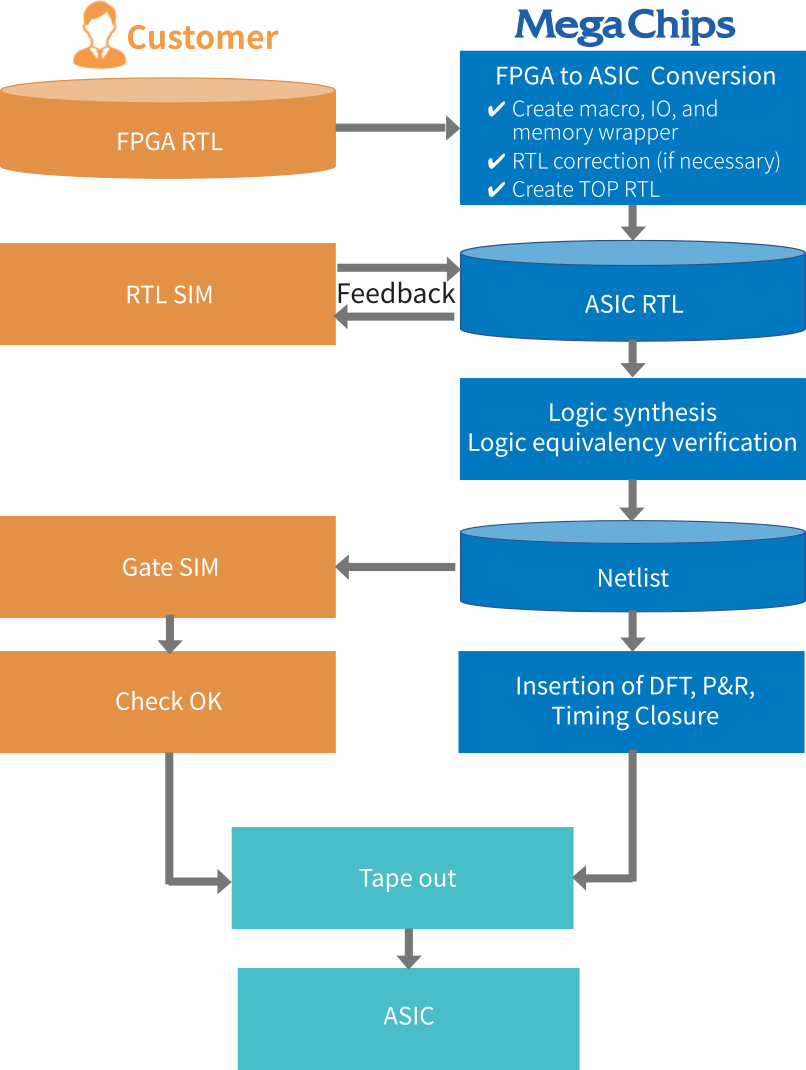
MegaChips listens to requests on existing FPGA assets and ASIC conversions, offering the best solution for ASIC conversion. We support pin compatibility with FPGAs as much as possible. The following is the process chart of the FPGA conversion to an ASIC. We can also be responsible for the logic simulation to reduce the burden on customers.
Development Process
Example of FPGA to ASIC Conversion Process
Customer Benefits
We have established a detailed support system from the beginning of ASIC design to mass production, which has been well received by our customers. We perform sufficient work and verify our operations while minimizing the burden on our customers until we use FPGA assets to convert to ASICs for mass production. The main advantages we offer to our customers are as follows.
Advantages
- Converting FPGAs to ASICs minimizes the burden on customers, but reduces costs during mass production.
- When the board design is completed, making ASICs pin-compatible with FPGAs can eliminate a modification of the board design.*
- Converting FPGAs to ASICs can reduce power consumption and, consequently, system power consumption.
- Thermal measures, like heatsinks, required for FPGA are unnecessary, which leads to cost reduction.
*As a result of a technological study, it may be judged that pin compatibility is impossible. We may also request improvements such as the addition of bypass capacitors.
Example of Development
Example 1: OA
| Item | FPGA | ASIC (55nm process) | Benefit |
| Development cost | JPY 30 million | JPY 80 million | Break-even point: 83K units |
| Unit cost | JPY 1,000 | JPY 400 | |
| Frequency | 200MHz | 200MHz | Equal due to FPGA conversion |
| Power consumption | 1300mW | 400mW | Reduced by 70% |
| Development period | - | 4 months from final RTL to ES delivery | - |
Example 2: FA
| Item | FPGA | ASIC (28nm process) | Improvement rate |
| Development cost | JPY 50 million | JPY 200 million | Break-even point: 15K units |
| Unit cost | JPY 10,000 | JPY 350 | |
| Frequency | 200MHz | 500MHz | Up by 2.5 times |
| Power consumption | 1000mW | 400mW | Cut by 60% |
| Development period | - | 8 months from final RTL to ES delivery | - |
Customer feedback
- Although we found unexpected RTL issues in our preliminary study of ASIC conversion, we were able to tape-out as scheduled with your scrupulous support.
- We had been considering mass production with FPGAs for a few years until the next ASIC model was launched. We switched over to ASIC conversion for cost reduction after receiving suggestions from you. It was a wonderful proposal.


