Solution (Application)
5G & Optical Communication
5G RU ASIC Solutions
Lower power and lower cost ASIC solutions for 5G RU
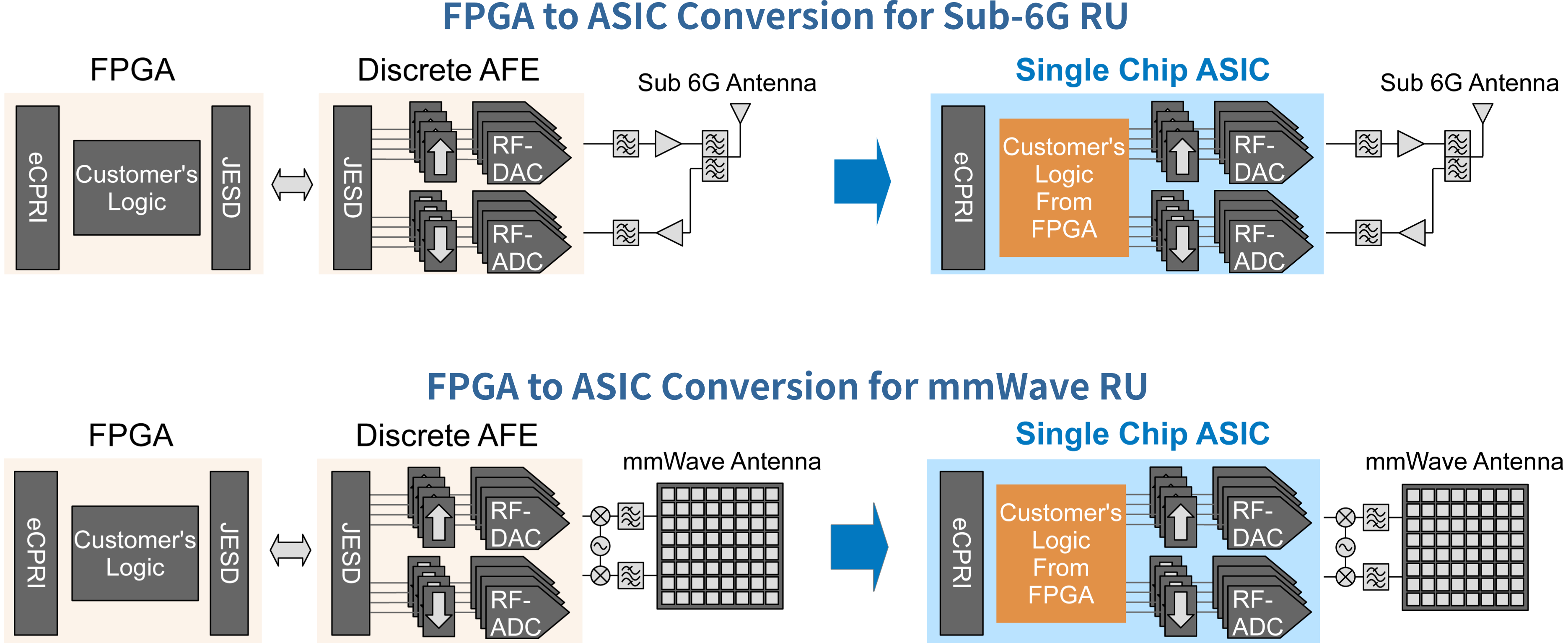
The “FPGA + discrete AFE” solution is the quickest way to build 5G RU system for proof-of-concept and/or early deployment purpose. However, there are challenges in terms of power consumption and cost. MegaChips 5G RU ASIC solutions, taking advantage of FPGA to ASIC conversion and high-end IP (like high-speed data converter) integration experience over the past three decades, enable lower power and lower cost 5G RU system for high-volume mass production.
Applications: 5G RU
- Sub-6G and/or mmWave macro cell
- Sub-6G and/or mmWave small cell
- mmWave smart repeater

FPGA to ASIC Conversion
Smooth conversion without compromising performance
FPGA to ASIC Conversion for 5G RU
MegaChips 5G RU ASIC solutions offer FPGA, which is a very power-hungry and expensive component, to ASIC conversion which enables customers’ system to be more cost-efficient and save power consumption up to 55% without compromising customer’s system performance.
To mitigate risks and make this conversion smooth, MegaChips offers two steps approach.
Step 1: Analog Test Chip Development
Ensuring analog IPs especially high-speed data converters work properly in the customers’ system at the early stage is a key to success of this conversion. For this purpose, MegaChips offers to develop the analog test chip which allows customers to test/evaluate analog IPs with their FPGA in their system. This will help to mitigate risks of unexpected performance of the final chip.
Step 2: Final Single Chip Development
Once the analog IPs’ performance/characteristics are confirmed at the system level test/evaluation, MegaChips converts user logic in FPGA to ASIC and consolidate it and the analog test chip into a single chip.
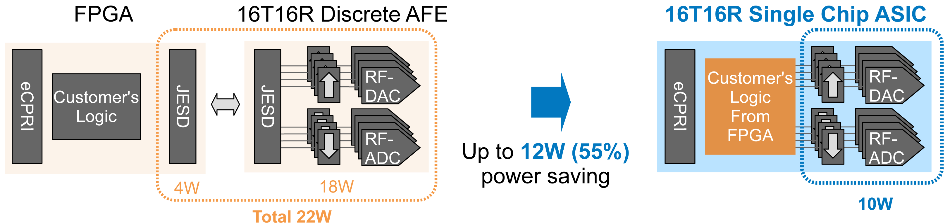
Up to 55% of Power Saving
Data bus between discrete AFE and FPGA significantly contributes to a large proportion of total power consumption and this proportion is growing because of the larger amount of RX/TX channels and/or massive MIMO. MegaChips FPGA to single chip ASIC conversion enables to save up to 55% of power consumption by eliminating this data bus.
| 16T16R DISCRETE AFE + FPGA JESD | 16T16R SINGLE CHIP ASIC IN 7 NM | ||
| FPGA JESD | 4W (250mW x 16 ch) | AFE | 10W |
| Discrete AFE | 18W (4.5W x 4 chips) | ||
| Total | 22W | Total | 10W |
Available Technology Nodes
TSMC: 28nm, 16nm FFC, 5nm or 7nm (planning)
GF: 22nm FDSOI, 12nm FDSOI (planning)
Comprehensive 5G RU ASIC Development Support
From Product Definition to Mass Production
Besides typical ASIC development supports like ASIC test/final chip development and ASIC production, MegaChips is offering development supports for the earlier development/design phases like production definition and FPGA development to customers who don’t have experience in chip development. This comprehensive support helps not only chip vendors but system/module vendors to add more value to their products and make it more cost-competitive.

Optical Communication ASIC Solution
The demand for optical communication is increasing at every level from backbone, metro, and access networks to home networks and terminals to support data communication that continues to rise along with the progress of AI, big data, and IoT. MegaChips provides solutions for high-speed interface and ASIC integration in the field of optical communications.
PON SerDes Technology
MegaChips has more than fifteen years of manufacturing experience in a high-speed serial interface (SerDes) for passive optical network (PON) optical access systems. The burst mode clock data recovery (CDR) SerDes technology, which we have accumulated over the years, can flexibly support a broad range of PON standards and is widely used within and outside of Japan.
The Idea of Upstream Signal Communication
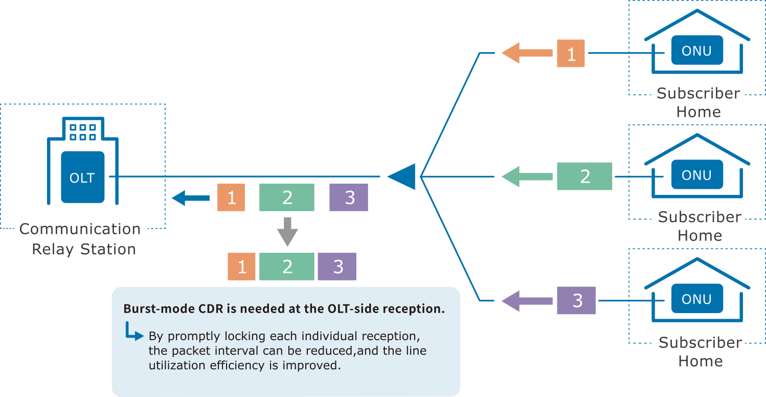
PON is a 1:N network that uses optical splitters to branch and connect communication relay stations and a number of subscriber homes. So, it is necessary for the upstream signal side to time split signals from multiple subscribers and receive them from one communication relay station. At the relay station side of the communication device (Optical Line Terminal (OLT)), the SerDes technology with a burst mode supported clock reproduction circuit that can promptly lock individual signals from different subscribers is demanded to enhance the efficiency of communication lines. From early on, MegaChips has been working on the commercialization of the burst mode compatible PON SerDes and has actively participated in international standardization.
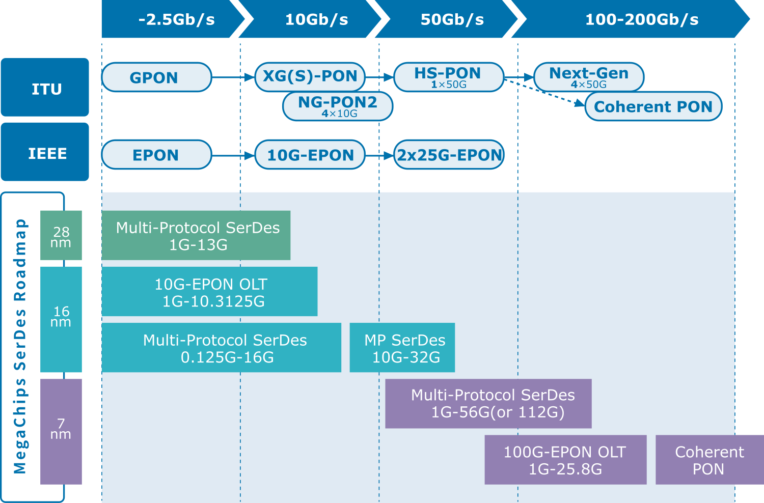
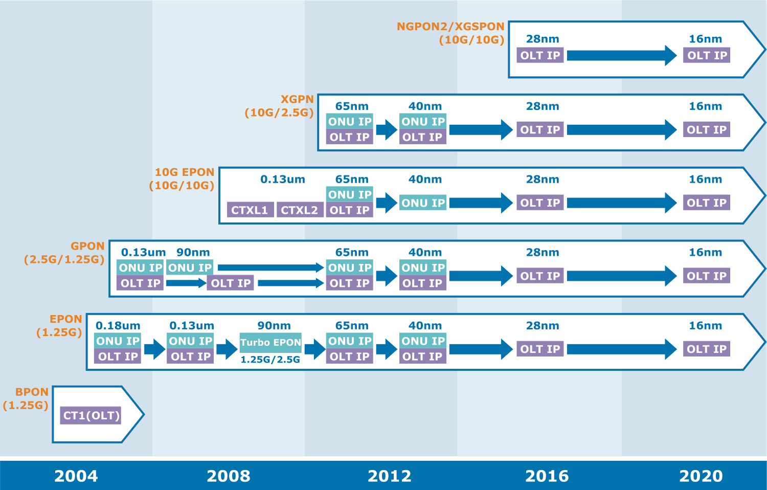
MegaChips PON SerDes History
MegaChips has provided a number of products for a wide variety of PON standards at both the relay station side optical line terminal (OLT) and subscriber home optical network unit (ONU).
Support for PON Standard Trend
MegaChips will monitor the trend of PON standards and provide ASIC products that satisfy customer needs.