Development Method and Flow
Design For Test
DFT
With the advent of the IoT era and the growing number of automotive electronic devices, higher-quality testing is becoming a more critical issue. In addition, ASICs are becoming progressively complex along with larger circuits, process shrink, and high-speed operations, increasing the requirements and design difficulties of design for test (DFT).
We have a large number of specialized DFT engineers familiar with testing and advanced EDA tools. The optimal design, depending on various projects, minimizes the impact on circuit scale and design TAT while achieving a low defect rate through high-quality testing.
Overview of DFT
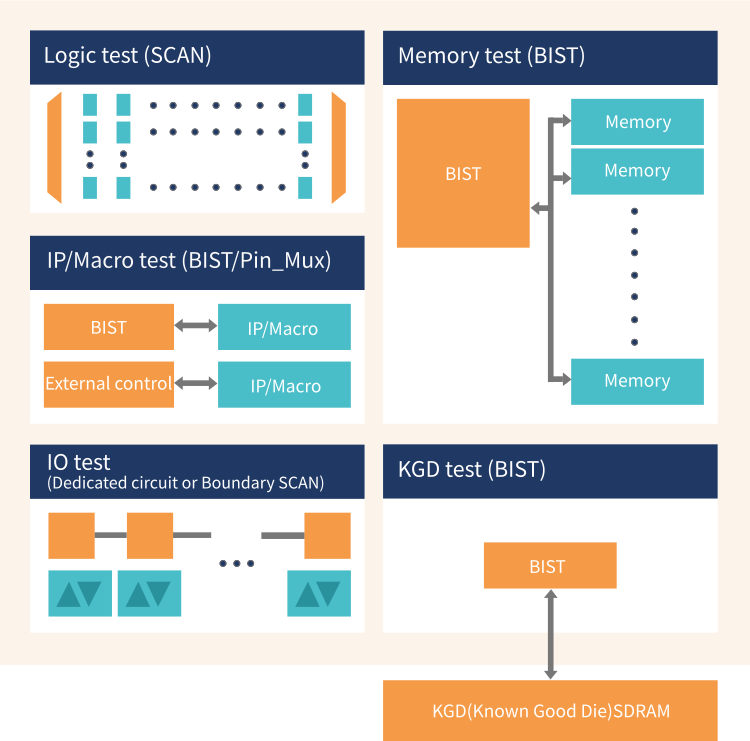
We combine standard parts in each project for building optimal DFT
Features of MegaChips DFT
Feature 1 : Support for High-Quality Testing
We use the following technologies to achieve high-quality testing.
■High-Speed Clock Testing Using On-Chip PLL
There is no need for the customer to modify the circuit for testing in advance regarding the preparation of a high-speed clock and the clock reset routing.
■Adoption of High-Level Fault Model
When necessary, the following high-level faults are taken into consideration during SCAN to achieve low defect rates.
- Cell-Aware (the fault nodes in cells)
- Bridging Fault (cable shorts)
- Path Delay (critical paths)
The FinFET supporting algorithm is applied in the Memory BIST to achieve low defect rates.
Feature 2 : Reducing the Burden on the Layout
The insertions to sophisticated DFT circuits can have negative effects such as area increase, timing convergence, and power growth during testing. To minimize these effects, we implement DFT insertions considering the layout when inserting SCAN and Memory BIST. In addition, for the mixed signal clocking system of the normal mode and test mode, we make detailed plans with layout engineers to achieve optimal circuit control and CTS.
Feature 3 : Acceleration of the Analysis of Defective Parts and Causes with a Dedicated Debugging Analysis Tool
With the increasing sophistication of testing, it is becoming more difficult to identify defective locations just from the fail logs. We can extract highly possible defective locations from the fail logs of mass production tests without needing to prepare additional tools of analysis. This reduces the time for the physical analysis and contributes to the cause analysis for field failure samples in a short time.


