
Development Method and Flow
Low Power Design
Low power consumption has become one of the most important points in ASIC design with the increase in gate size and the expansion of applications in mobile and IoT. The majority of power consumption in an ASIC is determined in the early stages of designing when formulating general methods such as operating voltage and voltage interruption. Therefore, method establishment can be described as the most important part, but it is exceedingly difficult to obtain the optimal solution due to a wide variety of alternatives. Through consultations with our customers, we develop optimal methods to achieve low power consumption.
Techniques and Measures for Low-Power Design
Proposal of Cell Library
Recent miniaturized technology offers many cell types, including multi-bit FF, and a wide variety of libraries consisting of multiple operating voltages, track counts, channel lengths, and Vth types. However, each block in a customer's circuit has different circumstances, some require high-speed operation, some accept low-speed operation, some have a high toggle rate, and some barely move at all.
With the application of situation-based cell libraries, occurrences of some trade-offs between leakage power and dynamic power, as well as some physical limitations such as power isolation and power routing resources, must be taken into account. Therefore, we share with our customers the block-level configuration of ASICs and the required specifications, suggesting a cell library to use and including a block division proposal.
Operation Stop, On/Off Consideration, Power Domain Settings
Other than stopping the clock, there are two ways for stopping the operation of the logic unit: a shut down for stopping external power supply, and power gating for stopping virtual power supply in a specified area. Also, there are three types of memory-stop operations: light sleep, deep sleep, and shut down. Each has advantages, disadvantages, and restrictions. After reviewing these items, we propose domain settings for optimal power and decide the implementation method by consulting with the customer. Customers may need to change the block configuration and verify logic related to the on/off operation.
Sample of Power Domain Settings
Build Optimal DFT for Each Project by Combining Standard Parts
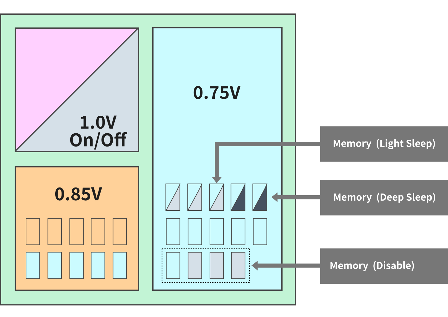
*The type and correspondence of the on/off function for memory differs depending on the memory type.
Proposals for Memory Cell Configuration
The amount of memory on ASICs can often be large, and memory power may account for the majority of power consumption. Therefore, low-power consumption for memory is particularly important.
For example, when a single-port RAM of 1K words × 32 bits is required, there are numerous memory type options (like a high-speed version, high-density version, register file), several Vth types, and various operating voltage selections, each of which have different bank numbers (aspect ratio). In addition, there is a configuration that can reduce power consumption by dividing word, thereby making the selection for the optimum solution not easy.
We search for optimal solutions from the above-mentioned candidates for multiple memory cells. At the same time, we consider the application of the power supply and the functions of light sleep, deep sleep, and shut down for the memory.
Low Power Function of Latest EDA Tool
We are building a design flow using advanced Cadence/Synopsys EDA tools and dealing with a variety of low-power methods supported by the UPF.
- External power shut off
- Power gating
- Multi-supply voltage
- Dynamic voltage and frequency scaling (DVFS)
- Automatic addition of level shifters and isolation cells associated with the above methods
- Highly accurate power estimate from RTL
- Consulting of RTL power reduction
In addition, we implement clock gating synthesis, the utilization of multi-bit FF, low power oriented data path circuitry synthesis, the optimization of dynamic/leakage power, cell layouts to shorten high-toggle nets, low-power CTS, and Vth swap to reduce leakage power in order to achieve low-power consumption at various stages of the design flow.
*Corresponding methods may vary depending on technology, libraries, and other conditions.
Approach to FD-SOI
A fully depleted silicon-on-insulator (FD-SOI) suppresses the leakage current and offers excellent power-saving effects, miniaturization, high performance, and low cost for various applications such as IoT that require low power.
We continue to strengthen our efforts on the FD-SOI and propose optimal ASICs tailored to our customers' needs.


