
Development Method and Flow
Overview
The development flow of MegaChips combines advanced EDA techniques with design kits and design services backed up by a wealth of experiences, making it possible to achieve optimal designs for customers in a short period of time. While continuing to evolve and improve everyday, we are supporting ASIC developments that are becoming larger and more complex.
MegaChips Development Flow
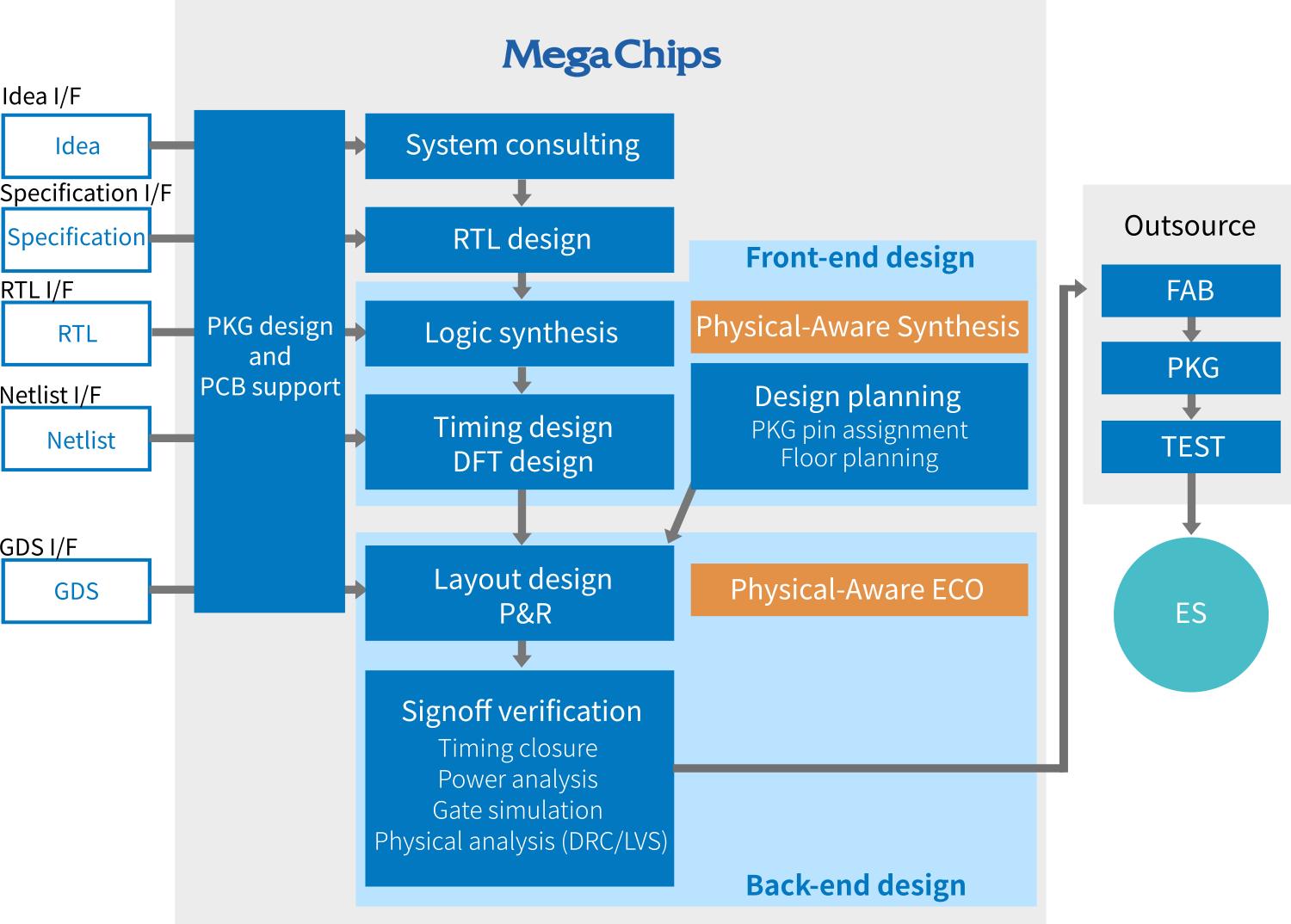
Front-End Design (Logic Design/Logic Synthesis)
We achieve optimal ASIC developments for power, performance, and area (PPA) in a short period of time with state-of-the-art EDA tools, optimized design environments, and design kits. We use our proprietary reinforcing tools and utilities to seamlessly connect each design process and prevent mistakes through rule checking.
Timing Closure
Timing closure is a key part of ASIC design flow. With the flow of completing an accurate SDC, ASIC implementation can converge quickly and securely, keeping the developing TAT adequate. We assign a full-time staff of timing closures when developing and securely inputting the increasingly complex timing requirements into constraint files (SDC). In addition, through careful reviews and smooth coordination with back-end designers, customers' requirements are accurately reflected in the design without omissions. Advanced physical-aware methods are incorporated into the design flow to minimize rework. Even large-scale and complex designs can be developed reliably and on schedule.
SDC Creation Support Utility
We have a proprietary SDC creation support utility. This allows one to create SDCs from Excel-formatted input files that one is familiar with. By managing timing specifications in intuitively easy-to-understand formats, high-quality SDCs are created in a short period of time, preventing miscommunications related to timing specifications.
Back-End Design (Physical Design/Verification)
As circuits become larger and more complex, the design periods grow exceptionally long in flat layouts, thereby increasing the need for hierarchical layouts. Leveraging industry-leading EDA tools and our extensive experience and performance, we have implemented hierarchical segmentation, the mapping of circuits, the connecting of signals and IO between hierarchical layout blocks, floor planning that takes signal flows into account, and P&R techniques on a block-by-block basis. Thus, greatly improving and shortening the design process and the time that it tends to take to complete.
Physical-Aware Synthesis/Physical-Aware ECO
With the miniaturization of transistors, designs that take physical data into account are the key to attaining optimal PPA without backward movement. We incorporate physical-aware synthesis/physical-aware ECO into our development flow and achieve early-timing convergence even for designs that are difficult to converge.
Physical-aware synthesis takes into consideration the physical data (P&R) during synthesis, and accurately estimates and improves the timing-violation points and wiring congestion issues identified after P&R in the synthesis phase. At an early stage, these difficult-to-converge issues can be fed back to RTL designs.
Physical-aware ECO performs highly efficient automated timing ECO through the consideration of pre-existing cell placement and the reduction of iteration to achieve early timing convergence.
Automatic Logic Correction ECO
When a complicated logic correction occurs just before the tape-out, it may lead to a drastic review of the development period. We use EDA tools to automatically generate logic correction netlists, which can be handled through an ECO without having to return to logic synthesis or re-layout, minimizing the schedule impact associated with the correction.


