
Development Method and Flow
Package Design
The engineers experienced in LSI design, RDL design, and mounting substrates will coordinate each and every package design by directly listening to the customers’ requirements. This creates a package design that maximizes ASIC performance when implemented in the customers’ system. As for the process from package selection to design, our manufacturing engineers and OSAT engineering department conduct scrupulous design reviews, consider design for manufacturing (DFM) and manufacturing simplicity, and aim for quality enhancement along with cost optimization.
Package Selection
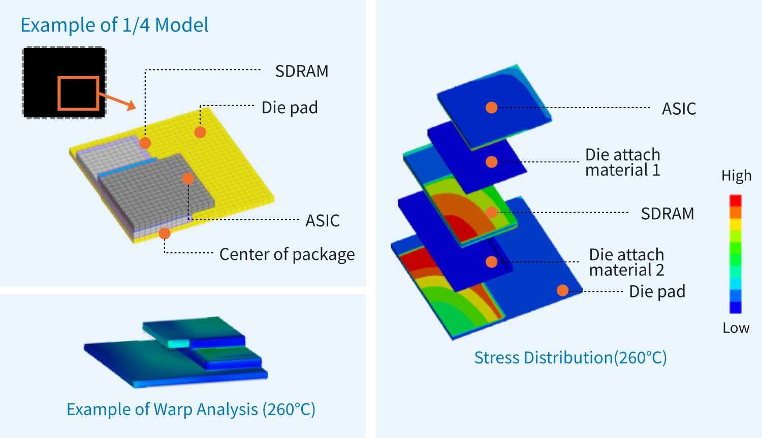
In the package selection, we compare various stresses on the silicon chip based on the structural analysis with our own criteria to prevent known trouble and enhance reliability. In addition, we conduct a warpage simulation at a high temperature to check the effect while mounting, as well as select the optimal package design and bill of materials (BOM).
Example of Warpage at a High Temperature and Stress Distribution in the SiP
Example of Thermal Analysis Combining the SiP and Product Enclosure
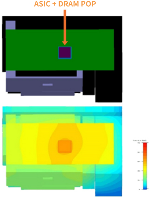
Example of product thermal analysis
Measurement/analysis condition
Ta=25℃
| Measured value | Analyzed value | |
|---|---|---|
| Tc | 59.1℃ | 61.2℃ |
Enables thermal analysis with in-depth modeling technology and precise power consumption.
With higher integration and a smaller package of LSI, it is becoming increasingly difficult to design systems that satisfy operating conditions with a conventional thermal design using package thermal resistance. Therefore, we select the optimal package by conducting a thermal analysis that combines the LSI, package, substrate, and enclosure.


